IG Electronics
Currency
0
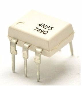
4N25

4N25 (Phototransistor Optocoupler IC)

BD 1.500
4N25 Features and Specifications
  • IR LED Forward Voltage for turning ON: 1.25V-1.5V (Typically 1.3V, 1.5V being absolute  maximum forward voltage)
  • IR LED Forward Current during ON: 10mA - 60mA (Typically 10mA, 60mA being absolute maximum forward current)
  • IR LED Reverse Voltage Maximum: 5V
  • IR LED Reverse Current Maximum: 100uA
  • Maximum voltage across COLLECTOR and EMITTER of TRANSISTOR: 70V
  • Maximum current allowed trough TRANSISTOR COLLECTOR: 100mA
  • Typical Rise Time: 2us
  • Typical Fall Time: 2us
  • No additional power needed to be applied for chip for making it work.


4N25 Equivalents

4N25 OPTOCOUPLER IC has many replacements like 4N26, 4N27, 4N28, 4N33, MCT2E, PC817. We need to check parameters and Pin configuration carefully before replacing. Replacing without taking voltage, current and frequency parameters may lead to permanent damage.


Similar Opto-coupler ICs

MOC3021 (TRIAC based OPTOCOUPLER used to control AC RMS voltage), FOD3180 (High-Speed MOSFET),


Why to Use 4N25 OPTOCOUPLER

For understanding the use of OPTOCOUPLER consider:

Case1: where you want to isolate LOAD CIRCUIT from CONTROL CIRCUIT. Say you want to control the speed of a small DC motor by using MICROCONTROLLER PWM output. This setup is not feasible as microcontroller is sensitive device. So for isolating load circuit and protecting the controller from voltage fluctuations we use OPTOCOUPLER.


Case2: Say you want to trigger a MOSFET circuit which is driving a high power load. The MOSFET trigger voltage typically is 12V. These voltages bursts (+12V) needed for MOSFET driver to control the high power load cannot be draw from controller. As controller puts out +3.3V or +5V bursts. In those cases using 4N25 OPTOCOUPLER chip is ideal.


Case3: Consider we want to switch a 12V relay which is looping 220V AC fan according to RASPBERRY PI outputs. It is ideal to use 4N25 in this case, as 4N25 draws negligible amount of power considering a transistor or a MOSFET.


How to Use 4N25 OPTOCOUPLER

4N25 OPTOCOUPLER IC has two components integrated in it. One is INFRARED DIODE and another of INFRARED PHOTOTRANSISTOR. The IR DIODE is connected between terminals 1 and 2, the PHOTOTRANSISTOR is connected at terminals 4, 5 and 6.The internal setup of two components can be seen below. The IR radiation emitted by IR LED will not be visible outside the chip. The whole issue of radiation will be working under background.

4N25 IC Internal Structure

For understanding the OPTOCOUPLER we will consider a circuit shown below.

4N25 IC Circuit

We will get the +3.3Voltage pulses from a microcontroller and these are driven to the POSITIVE of IR DIODE. When IR DIODE gets powered it will emit Infrared rays internally, when these rays fell on the PHOTOTRANSISTOR the transistor gets turned ON. When transistor gets tuned ON the current flows through load circuit and the voltage will be seen across the motor. Thus the motor rotates when microcontroller circuit provides HIGH logic to the 4N25 chip.

When the controller output goes LOW, the IR DIODE input goes LOW. With that the IR DIODE stops emitting radiation internally.  Since radiation is cutoff the PHOTOTRANSISTOR gets turned OFF since the radiation acts as BASE TRIGGER. So its LOW RESISTANCE state to HIGH RESISTANCE states. With HIGH RESISTANCE the complete supply voltage appears across the transistor and current flow in the load circuit gets ZERO. So the motor stops rotating. Thus the motor stops rotating when the microcontroller input to 4N25 gets LOW.

In this circuit you can see the motor draws power from the +12V battery source and not from the controller circuit. The PHOTOTRANSISTOR side secondary circuit here is in complete isolation with the CONTROLLER-PHTODIODE primary circuit. The resistors here are placed for limiting the currents in the circuit. Make a note the resistance values changed depending on voltages.


Switching Time of 4N25

Under normal circumstances you have no need to consider the SWITCHING DELAYS of 4N25 chip. These delays are the response time delays of 4N25. This timing only need to be considered when switching frequencies goes beyond 1MHz.

4N25 Switching Schematic and Timing

When the switching frequency goes higher, we need to take into account the two parameters of 4N25 in order to avoid the errors. These two parameters are RISETIME (tr+td) and FALLTIME (ts+tf). For understanding these parameters consider the circuit above as an example.

In here IF is the IR DIODE forward current. And Vo is the OUTPUT taken. Here Vo goes LOW when PHOTOTRANSISTOR is ON and Vo goes HIGH when PHOTOTRANSITOR is OFF. In another sense it is the voltage across the transistor and it represents the state of the PHOTOTRANSISTOR.

 As in graph, consider the IR DIODE is provided with power, the IR DIODE emits the radiation and PHOTOTRANSISTOR gets turned ON. But as you can see in the graph there is time delay between providing LOGIC INPUT and Vo going LOW at the OUTPUT. This delay in providing response is called RISETIME (tr+td). The RISETIME (tr+td) of the 4N25 is 2uS.

Similarly consider the IR DIODE power is cutoff, the PHOTOTRANSISTOR gets turned OFF. But as you can see in the graph there is time delay between LOGIC INPUT going LOW and Vo going HIGH at the OUTPUT. This delay in providing response is called FALLTIME (ts+tf). The FALLTIME (ts+tf) of the 4N25 is 2uS.

Here td and ts are in nano second so they are usually neglected.

Hence these time delay responses of 4N25 can get stacked leading to major errors. So during high frequencies one needs to take time delays into consideration.

Choose Quantity
+ Add to Cart
Product Details
Added to cart
- There was an error adding to cart. Please try again.
Quantity updated
- An error occurred. Please try again later.
Deleted from cart
- Can't delete this product from the cart at the moment. Please try again later.