
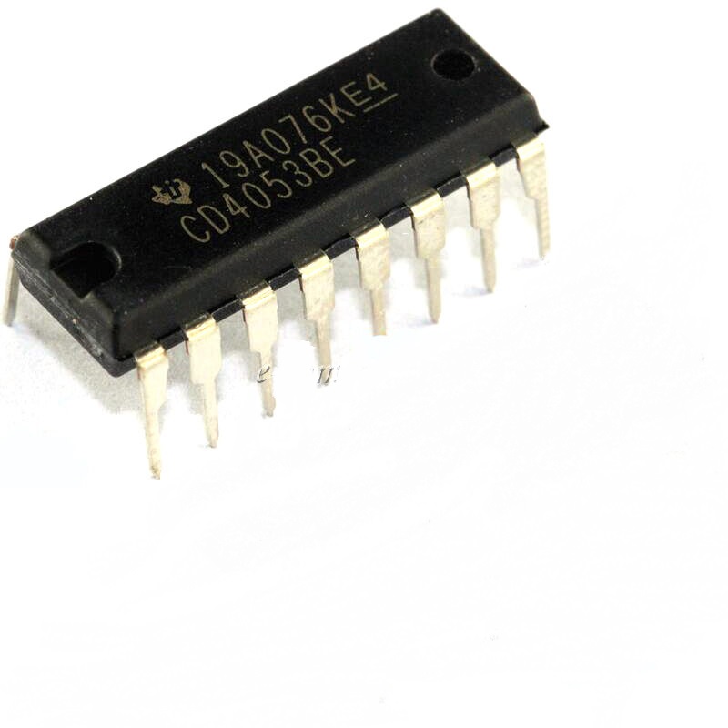
IC CD4053 (8-Channel Analog Multiplexer/Demultiplexer with Logic-Level Conversion)
BD 1.400
CD4051BMS, CD4052BMS and CD4053BMS analog multiplexers/demultiplexers are digitally controlled analog switches having low ON impedance and very low OFF leakage current. Control of analog signals up to 20V peak-topeak can be achieved by digital signal amplitudes of 4.5V to 20V (if VDD-VSS = 3V, a VDD-VEE of up to 13V can be controlled; for VDD-VEE level differences above 13V, a VDDVSS of at least 4.5V is required). For example, if VDD = +4.5V, VSS = 0, and VEE = -13.5V, analog signals from - 13.5V to +4.5V can be controlled by digital inputs of 0 to 5V. These multiplexer circuits dissipate extremely low quiescent power over the full VDD-VSS and VDD-VEE supply voltage ranges, independent of the logic state of the control signals. When a logic “1” is present at the inhibit input terminal all channels are off.
The CD4051BMS is a single 8 channel multiplexer having three binary control inputs, A, B, and C, and an inhibit input. The three binary signals select 1 of 8 channels to be turned on, and connect one of the 8 inputs to the output.
The CD4052BMS is a differential 4 channel multiplexer having two binary control inputs, A and B, and an inhibit input. The two binary input signals select 1 of 4 pairs of channels to be turned on and connect the analog inputs to the outputs.
The CD4053BMS is a triple 2 channel multiplexer having three separate digital control inputs, A, B, and C, and an inhibit input. Each control input selects one of a pair of channels which are connected in a single pole double-throw configuration.
The CD4051BMS, CD4052BMS and CD4053BMS are supplied in these 16 lead outline packages: Braze Seal DIP *H4X †H4T Frit Seal DIP H1E Ceramic Flatpack H6W *CD4051B Only †CD4052B, CD4053 Only
Choose Quantity
Product Details
Applications
• Analog and Digital Multiplexing and Demultiplexing
• A/D and D/A Conversion
• Signal Gating
* When these devices are used as demultiplexers the “CHANNEL IN/OUT” terminals are the outputs and the “COMMON OUT/IN” terminals are the inputs.
Features
• Wide Range of Digital and Analog Signal Levels
- Digital . . . . . . . . . . . . . . . . . . . . . . . . . . . . . . 3V to 20V
- Analog. . . . . . . . . . . . . . . . . . . . . . . . . . . . . . . ≤20VP-P
• Low ON Resistance, 125Ω (Typ) Over 15VP-P Signal Input
Range for VDD-VEE = 18V
• High OFF Resistance, Channel Leakage of ±100pA (Typ)
at VDD-VEE = 18V
• Logic-Level Conversion for Digital Addressing Signals of
3V to 20V (VDD-VSS = 3V to 20V) to Switch Analog
Signals to 20VP-P (VDD-VEE = 20V)
• Matched Switch Characteristics, rON = 5Ω (Typ) for
VDD-VEE = 15V
• Very Low Quiescent Power Dissipation Under All DigitalControl Input and Supply Conditions, 0.2µW (Typ) at
VDD-VSS = VDD-VEE = 10V
• Binary Address Decoding on Chip
• 5V, 10V, and 15V Parametric Ratings
• 100% Tested for Quiescent Current at 20V
• Maximum Input Current of 1µA at 18V Over Full Package
Temperature Range, 100nA at 18V and 25oC
• Break-Before-Make Switching Eliminates Channel
Overlap