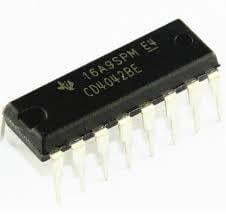
IC CD4042 (CMOS Quad Clocked D Latch)
BD 1.600
The CD4042 quad clocked "D" latch is a monolithic complementary MOS (CMOS) integrated circuit constructed with P- and N-channel enhancement mode transistors. The outputs Q and Q either latch or follow the data input depending on the clock level which is programmed by the polarity input. For polarity e 0; the information present at the data input is transferred to Q and Q during 0 clock level; and for polarity e 1, the transfer occurs during the 1 clock level. When a clock transition occurs (positive for polarity e 0 and negative for polarity e 1), the information present at the input during the clock transition is retained at the outputs until an opposite clock transition occurs.
Features
- Common Clock Input
- Low power TTL Compatible
- It gives normal and inverting Output (Q and Q’)
- Four Flip-flop Inside
- Available in both DIP and SOP Package
- Clock Polarity based controlled output
- Quiescent current specified up to 20v
Choose Quantity
Product Details
Technical Specifications
Applications- Input Supply voltage: 3v to 20v
- DC Input Current: ± 10 mA
- Input Capacitance: 5 to 7.5 pF
- Setup Time: 25 to 50ns (vary according to voltage)
- Hold Time: 50 to 120ns (vary according to voltage)
- Storage Temperature -65 to +150 °C
- Operating Temperature -55 to 125 °C
- Industrial
- Buffer Storage
- Holding Register
- general Digital Logic
